Jim Keller's startup is building a factory to mass-produce small chip fabs
Get the Tech newsletter
Daily tech — startups, AI labs, chips, the launches that shape the next decade. Free.
- Atomic Semi rebranded as Fab2 and moved to Texas, reframing itself as a "fab fab" that mass-produces small semiconductor fabs and the tools inside them
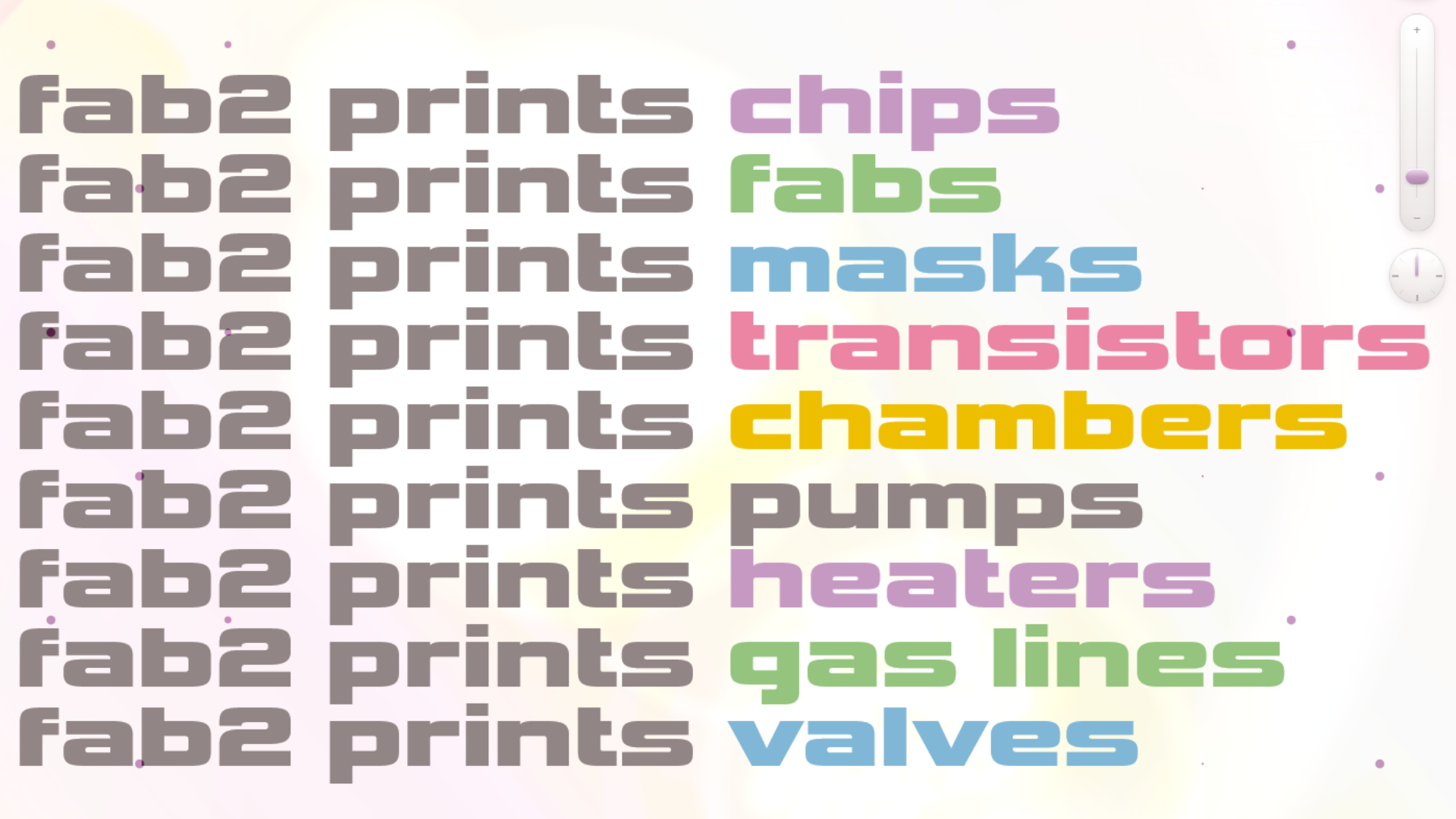
- Fab2 designs and builds every tool in its fabs in-house — pumps, valves, gas lines, lithography, and vacuum chambers — and pairs the hardware with Studio, a browser-based collaborative EDA tool for layout, schematics, and simulation
- The company uses electron-beam lithography to pattern sub-wafer chips and turn prototypes around in hours, a method that trades throughput for speed and is suited to prototyping and low-volume runs rather than commercial foundry production
- Fab2 operates three sites: a 120,000-square-foot Austin headquarters for research and production, a 30,000-square-foot "fab fab" facility in Lockhart, and the original 25,000-square-foot "garage fab" in San Francisco
- Co-founded in 2022 by chip architect Jim Keller and Sam Zeloof — who fabricated 300nm lithographic chips in his parents' garage as a teenager — the startup raised a reported $15 million seed round in 2023 led by the OpenAI Startup Fund at a ~$100M valuation, with ~84 employees as of May 2026
- Fab2's distributed small-fab model stands in contrast to Tesla and SpaceX's Terafab, an Austin megafab announced in March targeting a terawatt of annual compute at up to $119 billion — two competing answers to how the U.S. should expand domestic chipmaking capacity
Why it matters: Fab2's distributed model offers a second path for U.S. chipmaking — many replicable small fabs instead of consolidated mega-campuses like Tesla and SpaceX's $119 billion Terafab. The 84-person startup, backed by the OpenAI Startup Fund and Keller's track record, is built for prototyping speed, though its electron-beam lithography approach keeps it confined to low-volume runs rather than commercial production.